Tuesday 29 December 2015

Understanding how microprocessors work

Did you know that you are using microprocessors right now to view this very blog? Yes, the computer or smart phone device you are using to view this blog uses microprocessors as the very heart of the system. Today all automated machines whether servers, desktops or laptops all use microprocessors. If you are a gadget savvy person, you may have some idea of different microprocessors available in the markets currently like for instance, K6, Pentium, Sparc, PowerPC etc. While these are only different names for same device – all microprocessors perform similar functions.


While this big name ‘microprocessor’ might seem somewhat foreign; but you may be aware of the other name for it, CPU or Central Processing Unit. A CPU is basically a whole computation mechanism that is built on a single chip. The first microchip was introduced in 1971 and was called Intel 4004. Although it was not very powerful; but it could add and subtract only 4 bits at a time. But what was truly amazing about the device was that it was built with only one chip. Before the inception of Intel 4004, computers were built with collections of chips or isolated electronic components. Hence, something so nano-scale was truly inspiring for the entire electronic community. Although the 4004 powered computer was not really a full-fledges computer in comparison to the modern day devices. It was more like a new calculator that was portable.

To an average Joe how a computer works, may only be a wondrous imagination. But for those interested in digital electronics will find it interesting that all the amazing functions a computer does is base on simple digital logic, made to happen by design. Everything you do on a computer, from playing games, to listening to songs to spell-checking a document is controlled by a microprocessor.

The first microprocessor to have been installed in a home PC was the Intel 8080. It was a complete 8 bit computer contained in a single chip and was launched into the markets on 1974. But the real deal that made a huge splash in the whiz world was the Intel 8088 which was introduced in 1979 and included into the IMB PC that was launched on 1982.

The history of PC market goes on to move further ahead from 8080 to 80286 to 80386 to the Pentium processor, then Pentium II to Pentium III and then to Pentium 4. All these models were designed by Intel and are simply improvements made on the first 8080 model. The Pentium 4 can run any code that the 8080 could but only faster. 5000 times faster to be precise.

To learn more about digital electronics there are several online electronics training courses and other platforms where you can watch interesting electronics videos to expand your knowledge in electronics.
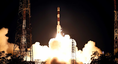
Related News


Sunday 20 December 2015

The pros and cons of video learning

The benefits of using educational technology and implementing video learning are numerous, but they also come with a few disadvantages. In today’s world most teachers are required to learn using educational technologies and to implement video tutorials in their lessons. In this blog we will go through both these aspects.

The pros and cons of video learning

My experience with educational technology in class:


The first time I used educational technology was in my first formal teaching assignment at college level. I still remember the day clearly; I was excited to use the most state-of-the-art technologies to teach an engaging topic to my class. The total strength of students were 23 and I was keen to get everything setup on time. So I walked to my class 5 minutes before the time of class, and a student waked beside me. He did not know I was the new teacher and casually said something that made my heart drop into my stomach and forced a cold sweat along my spine. “Did you hear? The internet is going to be down in this building today”, he had said. 

I’m sure many of you have had an experience with technology gone that is worth sharing. It is evident that when technology works well, it helps students to learn efficiently. But when there is a technical fault, it just creates utter chaos. The last time I tried setting up my router on my own, I asked my neighbor’s son (somewhat of those new-age whiz kids) to help me out. We ended up wasting our whole morning and afternoon trying to solve a tiny glitch that just seemed too stubborn to do away with. At the end of the day we had no new ideas except the one with restarting the whole system, including the PC. And voila! It worked.

So in my opinion, it is true that integrating technology with new computerized smart devices into academics can offer great benefits. But before doing so, it is necessary to train the teachers to be equipped to handle them. This will also help with schools good name as teachers will be able to answer unexpected questions from the students and parents and address technical issues with ease.


Pros of educational technologies in learning for students:


Are you a student of a difficult engineering subject? Having a tough time understanding circuit theory? You must have come across several platforms offering easy to understand electronics video tutorials on the internet. And I bet they helped solve your confusions. So why not use in class as well?

  • They help students be prepared for the future
  • Increase their motivation and engagement in class
  • Offers a wider access area with inspiring collaboration
  • Keeps them updated
Related News


Tuesday 15 December 2015

Have a career in electronics

There is a recent widespread belief that electronics engineering pass-outs and others pursuing electrical studies are losing demands in the job market. Is that so?

We aim to discuss the scope for people involved in studying electronics in terms of career prospects.
Have a career in electronics

What is electrical engineering about?

The field of electronic engineering deals with non-linear electronic components like, semi-conductors, electron tubes, integrated circuits, diodes, transistors, and other electrical components to build an electrical circuit which will form a part of a machinery system that can take care of certain mechanical or electrical functions. This can also be used to create passive electrical devices that are based on printed electric boards.

Electronics engineering field is a mother subject that encompasses several specific subjects like, analog electronics, digital electronics, power electronics, embedded electronic systems, consumer electronics and much more. This is one field that includes the implementation of principles, applications and algorithms that are related to various allied fields.

Career prospects for students with training in electronics and communications:

 The telecom industry is currently growing at a fast rate. As per the current statistics, the telecom industry accrues over 9 million new subscribers every month. Thus, it is safe to say that this creates a pretty large space for engineers with an electronics or telecommunications degree. Moreover, there is always the IT sector to look to, both hardware as well as software.

Currently, the nation is emerging to be one of hubs in the field of Embedded Systems or VLSI. The starting package for a quality engineer even at entry level positions could be around USD 6000.00 at the topmost MNCs around the world.

In fact the communications, media and entertainment industry is the biggest employer of electrical personnel around the world. A few big names amongst the leaders in the hiring industry are corporate biggies like Vodafone, Star network etc.

Some leading industries hiring B.Techs and others trained in electronics are:
  • Software engineering firms/IT
  • Telecommunications
  • Power sector
  • Television industry
  • Hardware manufacturing
  • Television industry 
  • Home appliance, VLSI design
  • Research and development

The job description in these fields mainly involves roles like setting up networks, maintaining electronic gears and other systems, setting up equipments. The list of biggest employers also includes names like IBM the corporate hardware giant, and other communications industry biggies like Siemens and Nokia also take up people skilled in electronics studies.

Related News


Tuesday 17 November 2015

How Manufacturers can Avoid Recall of Electronics

The ability to trace components of electronic instruments has assumed more significance than ever before and the trend is all set to continue. The end in mind is to curtail costs and liability due to recall and counter diversion and counterfeiting while continuing to maintain the brand’s integrity. This can be achieved by efficiently and effectively putting into use what is termed as data marking tech while manufacturing electronic components.

free electronics videos

Traceability Remains a Growing Need

When warranty claims related to recalls and defects are made, in ideal conditions the manufacturer would be to identify the origins of the parts to the specific process or machine. This may be attained through judicious and proper use of hardware and software. The task of the software in this particular matter is to come up with codes that are traceable whereas the hardware like cameras and printers are able to produce and authenticate the code involved.

An Upcoming Threat

The industry dealing with electronics is being challenged increasingly with electronics components that are actually counterfeits. In a recent article, the “Semiconductor Industry Association” revealed that electronic components counterfeiting costs the semiconductor industry by as much as $7.5 billion every year in terms of the loss in revenue. The unique coding method when applied on components and parts is exactly what the industry needed to provide necessary protection.

How to Put in Place a Traceability System

With the evolution of technology manufactures face the considerable hurdle on marking unique codes on components that are getting smaller by the day. In the absence of any single particular standard, some of the manufacturers are often required to mark specific codes by customers down in the buying stream.

The conundrum facing manufacturers of electronic components is how to implement a system of traceability that meets their unique and individual needs amidst a scenario of coding demand that is highly challenging.

The Options

Two marking and printing technologies exist that are well suited to meet such coding demands:


  • Laser marking systems
  • Continuous inkjet printers
Endwords

The latest breed of CIJ and laser printers may easily print in outstanding resolutions and prints of high durability and print in small spaces generate all sorts of complex codes; providing a solution to the problem of implementing traceability systems. online electronics training will get you all the know how needed to understand the basics of electronics and comprehend the issues dealt with in this post all the more.

Related News


Tuesday 6 October 2015

Top 5 Technologies for Sustainable Development

In the present years, during the advent of Electronics training, the exact technologies to make improvement sustainable are accessible. In this connection the major challenge is to make connections between the general population with the thoughts, those taking a shot at the ground with the local information on how it may function and the investors to support them.

 Top 5 Technologies for Sustainable Development

Here, I am going to incorporate some inventive, fresh technologies which are the leaps forward in pushing new limits.

Algae Biofuels

12% of flight fuel could originate from green growth by 2030, if monetary reductions don’t mediate. In 2009, the primary green growth fuelled car was put out and about. Green growth fuel, a fluid seeming to be like vegetable oil, discharges the carbon’s fifth outflows of fossil fuels and could be prepared in proficient seaside lakes.

Zinc-air Batteries

With world assets of zinc being 100 times more ample than lithium particle, a shift to zinc-air batteries can possibly make computers more versatile, electric automobile more reasonable and portable amplifiers more solid. Zinc is ecological, moderately cheap and great source of energy.

Natural Solar Cells

As per UK’s Carbon Trust, inexpensive natural sunlight based cells can be made sufficiently effective to prevail business achievement. But, expectations have been disillusioned repetitively as makers are yet to get above 9% change from light to power. However, in the event that leaps forward happen, a considerable lot of us will begin wearing sun based apparel, conveying sun powered umbrellas and utilizing versatile sunlight based chargers.

Sea Energy

The US, UK, Norway and Canada are in front for creating tidal energy and ocean wave assets, however, expenses are still generally twofold what is financially suitable. A scope of development is being produced, especially in the more progressed and less exorbitant region of tidal forces. The Carbon Trust appraises that 20% of UK power needs could be met by the ocean from the 2020s.

Smart Lighting

Smart lighting is an affluent range of technology with several little associations, growing better approaches to supply poor nations with sun oriented lamps, or, on the flip side of the range, to give inhabitance sensors and sunlight delicate schemes for industrial units. Lights that monitor biochemical perils or which can give web access are in the pipeline.

Presently, it is vital that we move this talk without hesitation and start to allocate the basic technologies that will enhance lives far and wide.

 Related News


Wednesday 30 September 2015

Isro Launched First Satellite Astrosat

Isro, on Monday, effectively propelled first astronomy satellite of India, Astrosat - after 11 years the legislature cleared the task. 

Isro Launched Its First Astronomy Satellite Astrosat

At 10am, Astrosat, conveyed by a Polar Satellite Launch Vehicle (PSLV-C30) and six different satellites detonated from the Satish Dhawan Space Center in Sriharikota.

After liftoff, in around 25 minutes, PSLV-C30 infused Astrosat and different satellites, which include four nanosatellites of the US, an Indonesian microsatellite and a Canadian nanosatellite - into their separate courses. For the first time India is propelling a US satellite.

644.651km from earth Astrosat was put on a course, as wanted. The satellite accomplished a normal slant of 6.002 degrees.

P Kunhikrishnan, the director of Satish Dhawan Space Center, said after the dispatch, that the mission is fruitful. It is an all around perceived and synchronous endeavor. For him it was a well deserved blessing.

About Astrosat:

Astrosat, having a takeoff accumulation of 1,513kg, now will set out on a five-year cosmic operation concentrating on inaccessible divine articles.

It will monitor the universe in the bright, ocular, high and low energy x-beam areas of the electromagnetic range, contrasted with nearly all other exploratory satellites that are fit for watching a wavelength band’s restricted scope.

In the middle of its assignments, Astrosat’s 5 payloads will learn black-holes and star conception locales.

The website of ISRO records out the observatory’s target - to see high vitality forms in twofold star frameworks containing black-holes and neutron stars; to gauge magnetic grounds of neutron stars; to read star conception areas and lofty energy forms in star frameworks lying past the galaxy; to identify new sources for temporarily brilliant x-beam in the sky and finally to execute constrained profound ground-overview of the ultraviolet locale of the universe.


Astrosat, conveying 5 payloads, is equipped for watching the sky in the perceptible, close UV and far UV areas of the electromagnetic range.

There are two telescopes on the Ultraviolet Imaging Telescope (UVIT) payload, which are intended to accomplish a magnificent picture determination, whereas the other 4 payloads have their particular parts.

Alternate payloads are – Soft x-beam Telescope (SXT), Large X-Ray Proportional Counter (LAXPC), Charge Particle Monitor (CPM) and Cadmium Zinc Telluride Imager (CZTI).

On next Monday, the payloads will begin taking a shot, on the eighth day after dispatch.

 Related News

http://www.techtimes.com/articles/54828/20150522/scientists-develop-light-emitting-paper-that-might-shape-future-of-bendable-electronics.htm


Monday 24 August 2015

Study Says Saturn and Jupiter were Small as Pebbles

There have been many studies and researches around the mystery of emergence of gas giants such as Saturn and Jupiter. According to a recent study, the researchers are finally successful in deciphering the mystery and have found this - Saturn and Jupiter possibly have been started forming before 4.5 billion years generated from the small pebbles measuring to centimetre emerging from dust and ice spinning around the newborn Sun. 

Study Says Saturn and Jupiter were Small as Pebbles

By swiftly melding into the nuclei, the primeval pebbles had turned into Jupiter, Saturn and other gas giants. According to the previous researches, a splendid cluster of much-bigger chunks is required for constructing a giant planet, with the distance of a kilometre between each chunk.

However, for the scientists it was difficult to find any explanation regarding the plausibility of the completion of this process of turning the pebbles into gas giants in only some millions of years; even before dispersion of the disk of dust around the Sun.

According to a report by ‘Nature’ in 2012 Michiel Lambrechts and Anders Johansen of Lund University in Swedens were successful in solving this notion of pebble-accumulation. According to their study a substantial explanation was able to find out about how a terrestrial core could form that fast, whilst abrasion between gas and the disk would have slowed down the process of accumulation of the pebbles into a sprouting planet.

The theory drawn by Michiel Lambrechts and Anders Johansen showed that through simulations it is possible to create hundreds of substances similar to that of the Earth, flying around the Sun. This theory has abolished the idea of ten times larger objects than the size of Earth and few in amount which previously have been thought to be the nuclei formation of the giant planets.

Another planetary scientist, Harold Levison of Southwest Research Institute in Boulder has declared that there are simulations possible for allowing more time to growing planetesimals to intermingle and smash with each other. Depending on the primary conditions, the simulations of this research team have usually occurred between one and four of the gas giant planets, like Jupiter, Saturn, Uranus and Neptune.

Monday 10 August 2015

OBAMA BACKED REPLACEMENT PART RECOGNITION APPLICATION

On Tuesday, 4th August of 2015 a conversation was held with the president Barak Obama at the White House for a Demo Day where the entrepreneur from Atlanta, Ga., Jewel Burks had the most precious chance of conversing regarding her initiative of Partpic.

OBAMA BACKED REPLACEMENT PART RECOGNITION APPLICATION

Jewel Burks along with the co-founder Jason Crain explained the ways they came up with the idea of launching Partpic which is an application developed for the purpose of helping companies recognize and order the exact replacement part for getting back their machines’ functionality.

From her experience of working in a parts call center and her childhood occurrence of helping her grandfather into getting a replacement part for his tractor helped her to turn up with the idea of this company. Her desire to help people out in searching for the part needed for their machines is what that drives her into this endeavour.

What was most inspiring for Burks, the President showed genuine interest in understanding the comprehensive details of the company. At the Demo Day, Burks’s company was one of the 30 start-ups and 90 entrepreneurs who were all invited to take a role in the initiative taken on the part of the administrative that will encourage many to include in the tech industry.

Obama cited that if the companies on a global scale continue to put stress in employing diverse leadership, there will create more scope for opportunity. The lack of participation is possibly the reason that the companies are not doing good. In this occasion Obama had been more particular in mentioning that women CEOs are employed in less than 3% venture capital-backed companies, at the same time, less than 1% companies have an African American as their founder.

The president announced that miscellany initiatives will be taking place with new public-private tech firms along with more than 40 leading venture capital firms for the purpose of increasing varied practices for hiring and funding. The co-founder of The Electronic Frontier Foundation and his wife Freada Kapor have committed a $40 million investment for the development in the tech sector.

Adding to the success of Obama’s administration, over 100 engineering schools have pledged to TechHire initiative that will focus on diversity hiring and more comprehensive student enrolment. 

 Related News

Friday 7 August 2015

Flexible Paper can Emit Light

Since the first emergence of technology, the evolution never stopped.And now in the present age of rapid advancement of smart gadgets another extraordinary collection has been added into the list of smartproducts – the firstever light-emitting, transparent and flexible paper. 

 Bendable Technology with Light-emitting Flexible Paper


The evolution of smart technology added many gems into its list – from phones to tablets and then watches and glasses. However, these inventions could not eradicate the barrier of rigidity. Now the Researchers from China have reported that they have developed light-emitting, transparent and flexible paper – a technology that takes one step ahead to the revolution of bendable electronics.

This transparent, flexible and light-emittingpaper is reported to be environmentfriendly that has been made out of similar eco-friendly materials using a simple anda greater rate of filtration technique.

It has been long predicted by the technology experts that the age of flexible electronicsis coming, and researchers are working diligently on severalfacades to find a way towards that goal. Sincemost of the progressesdepend on petroleum-based plastics and toxic materials, Yu-Zhong Wang, Fei Song and their colleagues in China wanted a solution in a “greener” way.

In this endeavor, Yu-Zhong Wang and Fei Songled a team of researchers who were material scientists at Sichuan University, China. About the research and the outcome have beenissuedin the American Chemical Society's journal Applied Materials and Interfacesthis week.


What thescientists wrote in their new paper is pretty inspiring, "This material can bring a new thinking on future electronic displays and 3D printing papers". The paper that the researchers developed is a thin, clear nanocellulose paper prepared out of wood flour and later suffused it with biocompatible quantum dots. These arelittle, semiconducting crystals which are made combining zinc and selenium. What is interesting is that this paper glows at room heat and can easily be rolled and unrolled without the fear of cracking it.

 Related News

http://www.techtimes.com/articles/54828/20150522/scientists-develop-light-emitting-paper-that-might-shape-future-of-bendable-electronics.htm

Wednesday 5 August 2015

In Collaboration with Micron Intel Launched 3D XPoint Memories

On the 28th of July, 2015 in London, the company executives of the Intel and Micron Technology launched the first category of memory that is described by both the companies as a major development after 1989 when the NAND flash was first emerged. It is the 3D XPoint memory IC with 128Gbits capacity which according to a primary finding is a fixed memory that reveals a massive capacity for material property change where the metal access lines meet at a cross-point.

What you need to know about vaping hazards of E-Cigarettes


The buzz is already around the electronics industry that this memory may possibly bring a major revolution. It is hoped that this memory will be faster up to 1000 times than NAND flash. Also the density of the memory is 8 to 10 times more than DRAM, making the cost relatively low. The applications of 3D XPoint memory are predicted to be lucrative for the data centers and the solid-state drives.

According to the CEO of Micron Mark Durcan that this is the result of the joint venture between Intel and Micron built in 2006. It was being produced at the wafer fab in Lehi, Utah, which belongs to IM Flash Technologies LLC. The Micron CEO further enforces that the memory is structured in a way that it will remain as two planes of 64Gbits where one bit will be quantified for each cell.

The engineering details were disclosed at the launch event as well. According to the Intel and Micron while creating the 3D XPoint memory they were stressing on inventing material compounds that will be unique in nature. They did not disclose much about the switching mechanism but hinted that it is by means of modifications done in resistance of the bulk material.


There are similarities of 3D XPoint to ReRAMs developed by Crossbar Inc. as it is a resistive RAM with a select integral diode making an opaque structured device. But it has been confirmed that 3D XPoint cannot be pertained and comparing to other forms of stable memory, the 3D Xpoint is fundamentally a special switch made for bulk-switching mechanism. 


Related News

http://www.c-sharpcorner.com/News/4965/intel-and-micron-collaborate-to-launch-3d-xpoint-technology.aspx

Monday 27 April 2015

The Fate of Future Electronics Lies on Carbon Nanotubes


The unique properties of Carbon Nanotubes, the tiny molecular cylinders, have enticed researchers for years because of the possibility that they could serve as the successors to silicon serving as the electronic devices that are smaller, faster and cheaper.

First, they are tiny on the atomic scale and perhaps close to the physical limit of how small you can reduce a single electronic switch. Like silicon, they may be of semi-conductive nature, which is essential for the circuit panel, and they may endure very rapid and controllable electrical switch.
Source: http://goo.gl/Uim7L4

But the major obstacle to useful electronic construction out of carbon nanotubes has always been that when they are placed in films, few parts of them act more like a metal than a semiconductor. This defect can spoil the entire film.

In effect, Professor John Rogers of University of Illinois professed that purity must exceed 99.999%, i.e. even a bad tube in 100,000 is enough to kill an entire electronic device. These kinds of materials will not work for semiconductor circuits.

Currently Rogers with the help of a team of researchers have experimented using rather easy, scalable method that does not involve costly tools to strip out the metallic carbon nanotubes from assortments.

Benefits of Carbon Nanotubes:
Carbon Nanotubes have multiple exceptional advantages, comprising of:
  • High thermal and electrical conductivity
  • Optical properties
  • Flexibility
  • Increased rigidity
  •  High tensile strength (100 times stronger than steel by weight)
  •   Lightweight

Applications of Carbon Nanotubes:
  • At present Carbon nanotubes are applied in different products, and researchers are looking forward to discover new creative applications.
  • Current applications include:
  •   Bicycle components
  • wind turbines
  • Flat screens
  • Scanning probe microscopes
  • Detection devices
  • Electrical circuits
  •  Electronic and many more
  • Future uses of carbon nano tubes are quite interesting which include:
  • Stab-proof and bullet-proof Clothing
  • Semiconductor materials
  • Spacecraft
  • Space elevators
  • Solar panels
  • Cancer treatment
  • Touch screens
  •  Energy storage
  •  Optical technology
  • Radar
  • Biofuel 
  •   LCD
·         Submicroscopic test tubes
CNTs are very new material with little continuing history. Although no human has yet fallen ill due nanotubes, nevertheless scientists urge caution while handling nano particles. The potential health risks are not cause for alarm and the future of Carbon Nanotubes is quite bright in the world of electronics